Debugging a faulty PCB
One of my ongoing projects is home-brew home automation and environment sensing. I’ve made some sensor nodes that are placed in each room and they record environment data (temperature, humidity) that is transmitted to a central server that displays the readings on a little graph. At some point I’ll do a write up of the overall system but for this post I want to talk about the sensor nodes and my first attempt at a circuit board for them.
Sensor Node PCB Design
The nodes use the Raspberry Pi Pico W platform which is connected to various sensors (BME280, MMA8653) as well as an EEPROM (24LC04) for storing configurations. The schematic I designed is shown below, which also shows connectors for additional user IO (GPIO A, GPIO B) as well as a jumper for putting the Pico into “Config mode” where the user can program various settings.
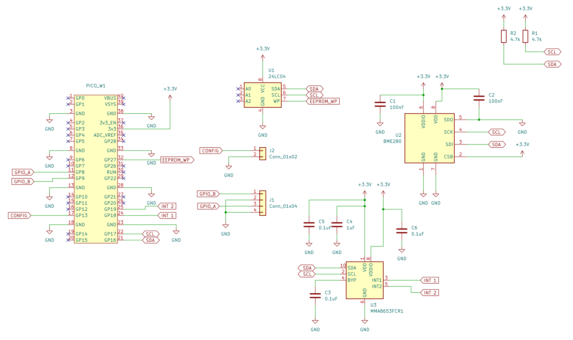
Picoboard schematic
Following this I got a PCB designed and manufactured with the end result pictured below. I’d opted for headers so that I could swap out Picos should one be faulty or should I want to change the platform.
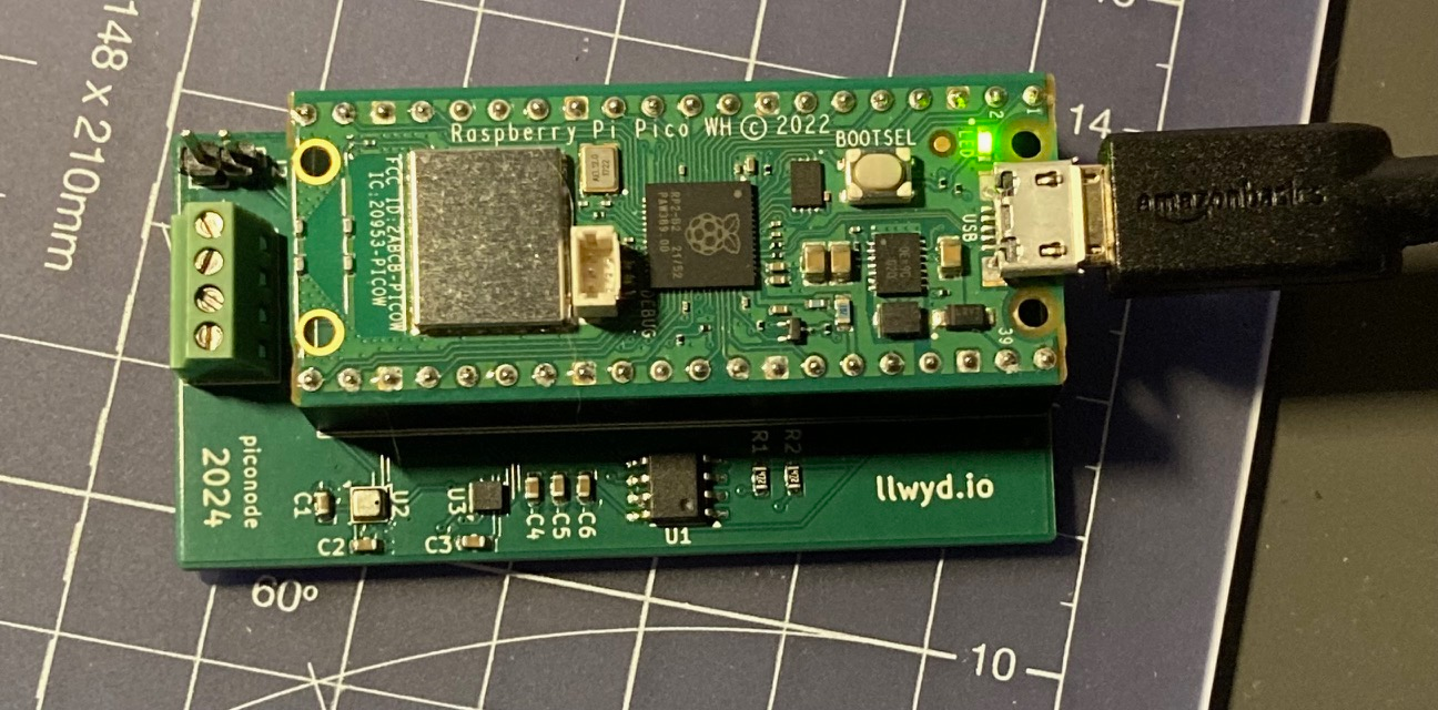
End result with a Raspberry Pi Pico W inserted
Does it work?
Upon receiving the circuit boards it was time to test which components worked. I summarised the individual functionality in the following table along with the result of whether it worked or not.
| Functionality | Pass/Fail |
|---|---|
| BME280 Environment Sensor R/W | PASS |
| Accelerometer R/W and GPIO | PASS |
| EEPROM R/W | FAIL |
| GPIO A | PASS |
| GPIO B | PASS |
| CONFIG Pin | PASS |
The tests showed that everything worked except the Read/Write of the configuration EEPROM, time to investigate!
Fault Finding
When the picoboard is in Config mode it supports a very basic command line interface so that I can configure various settings which are then stored in the EEPROM. When attempting to read the stored configuration I was met with errors on the I2C bus as shown below.
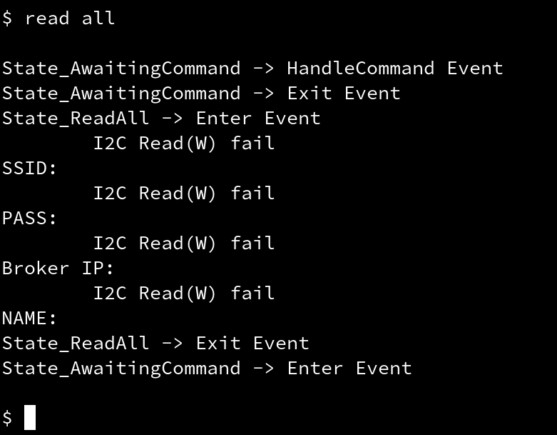
CLI showing EEPROM read failures
Given that the accelerometer and the environment sensor were both on the same bus and worked successfully I ruled out there being any issue with the I2C driver code as well as the choice of pull up resistors. I decided to connect a logic analyser to see what was happening on the I2C bus.

Logic Analyser showing I2C address NAK
The logic analyser revealed that upon sending the initial address that it received a NAK instead of continuing with the rest of the transaction. I decided to check the data sheet again and verified that the address was correct. Having scoured the data sheet I went back to my schematic and noticed I’d made a mistake in my design.
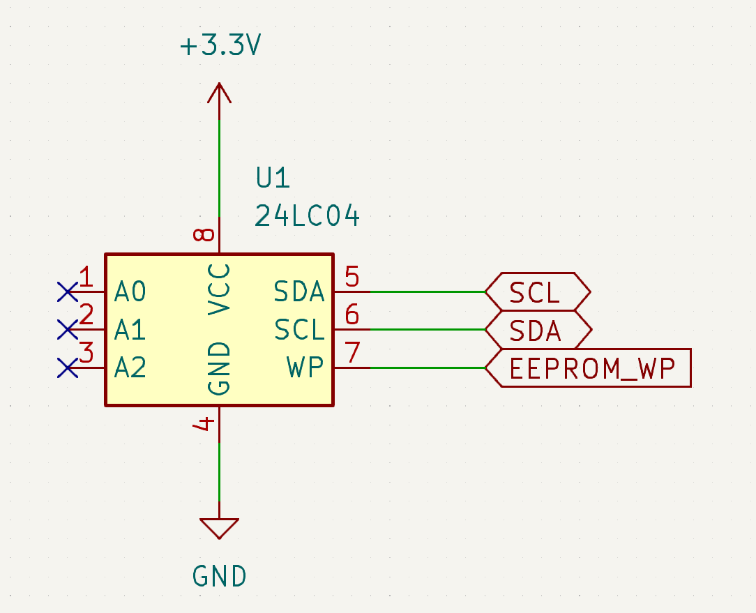
Woops
I had got the SDA and SCL labels the wrong way round!!! A careless mistake on my behalf. I modified one of the circuit boards so that the SDA and SCL lines from the Pico were swapped round and retried my EEPROM tests.

Logic Analyser showing I2C address ACK
The logic analyser was now showing that the address as being ACK’d by the EEPROM, allowing the rest of the transaction to continue.
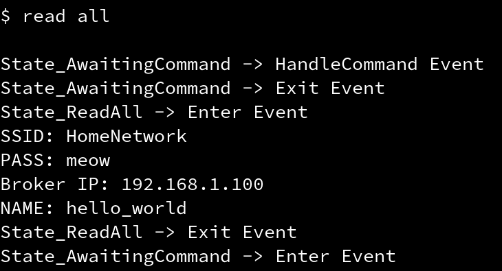
CLI showing EEPROM read success
The CLI was showing the values I’d written to the EEPROM! Result!
Conclusion
A minor but nonetheless embarrassing mistake but easily identified with help from a logic analyser!